
HOME
MY PAGE


イベントトップに戻る
セミナースケジュール
Dec.11_9:30_STS計測・検査セッション
STS計測・検査セッション
先端デバイス向け計測・検査技術の最新動向
2026/12/11(金) | 09:30 - 11:30
東8ホール 商談室(1)・(2)および オンライン(Zoom)
参加費(税抜き価格)
| SEMI会員 | 一般 | 学生 | |
| 早割(10/7〜31) | 8,000円 | 16,000円 | 4,000円 |
| 通常(11/1〜) | 10,000円 | 20,000円 | 5,000円 |
※講演資料 事前ダウンロードリンク付き
- お申込み後のキャンセル・変更・および返金は一切お受けしておりません。お申込みの前に必ずこちらの確認事項をご一読ください。
- 学生の方は来場登録の方法が異なります。こちらの内容を事前にご確認の上、お申込みください。
- 対面/オンラインでチケットが分かれております。またオンライン向けEarlyBirdチケットのご用意はございません。お申込みの際にはご注意ください。
半導体デバイスの微細化・3次元化に伴い、高精度な計測・検査技術の重要性がますます高まっています。AIなどを活用した寸法・形状計測や欠陥検出・異常予測など、歩留まり改善への貢献が期待されています。本セッションでは、先端デバイスおよび先端パッケージ分野における計測・検査技術の最新動向と将来展望をご講演いただきます。
※プログラムは都合により変更となる場合がございます。予めご了承ください。
プログラムアジェンダ
セッションチェア:
中村 肇(オントゥ・イノベーション・ジャパン)
堀田 尚二(日立ハイテク)
浅野 昌史(東京エレクトロン)
山崎 裕一郎(東レエンジニアリング先端半導体MIテクノロジー)
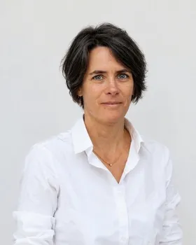
Metrology and inspection (MI) have been at the heart of semiconductor manufacturing for more than four decades, evolving from standalone measurement tools into a broad ecosystem of technologies and data-driven solutions. However, as the industry enters the Angstrom Era, new technologies such as High-NA EUV and 3D device architectures, are creating extra levels of complexity and are challenging conventional approaches. At the same time, beyond traditional process control, MI is becoming a key driver of innovation, helping accelerate technology development and improve understanding of increasingly complex processes. In this talk, we will explore the major metrology and inspection challenges facing future logic, memory, and advanced packaging technologies, and review recent innovations that are helping address them. We will also discuss how metrology and inspection are evolving to support the next generation of semiconductor breakthroughs and what will be the requirements to enable the transition from innovation to high-volume manufacturing.
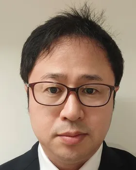
フラッシュメモリは最初に平面での縮小化による高密度化の技術限界に直面したが、積層型の三次元構造を導入することでこの限界を打破してきた。本講演では、三次元構造を採用することにより生じた検査計測の課題と、それに対する解決策となる検査計測技術について紹介する。

This presentation examines the metrology and inspection challenges of heterogeneous integration, with a focus on hybrid bonding as the technology where those challenges are most acute. Sub-micron bonding demands tight control of overlay and die-placement accuracy, bond-interface integrity and void detection, CD and profile at shrinking pad pitch, and warpage across wafer- and panel-level formats-parameters that no single inspection modality can fully resolve. The talk addresses the complementary roles of optical, X-ray, and electron-beam techniques in providing visibility into buried structures, interfaces, and defects, set against the broader context of fine-pitch RDL and 3D integration. It closes with an outlook on the process-control requirements and inspection innovations needed to keep pace with future heterogeneous integration architectures.
ご希望の方は、セミナー終了後もそのまま会場にお残りください。
ドリンク・軽食をお楽しみながら、講演者や参加者の皆さま、関連出展企業との交流を深めていただけます。 本セッションご登録者の方であれば、どなたでもご参加いただけます。お時間になりましたら来場者バッジをご持参のうえ、直接会場へお越しください。