

HOME
MY PAGE


イベントトップに戻る
セミナースケジュール
Dec.9_15:10_Global Semiconductor Leadership Summit 2
日付 > Dec. 9
セミナーカテゴリ > SuperTHEATER
セミナーカテゴリ > 政策・市場
セミナーカテゴリ > 翻訳サポート
Global Semiconductor Leadership Summit 2
AI時代を支える半導体エコシステムの進化と競争力

2026/12/9(水) | 15:10 - 17:00
SuperTHEATER(会議棟1F レセプションホールA・B)
無料
翻訳サポート
 日英翻訳サポートをご利用希望の方
ご自身のスマートフォンおよびイヤホンをご持参ください。
※詳細はFAQをご確認ください。
AIの進化とともに、半導体産業では設計・製造・テスト・実装に至るまで、エコシステム全体で技術革新が加速しています。これまで以上に各分野の連携が競争力の鍵となり、次世代半導体の実現を支えています。本セッションでは、AI時代の半導体イノベーションをはじめ、プロセス技術、テスト技術、先端パッケージングなど、半導体エコシステムを支える最新技術と今後の方向性を紹介し、グローバル競争における競争力強化の鍵を探ります。
※プログラムは都合により変更となる場合がございます。予めご了承ください。
プログラムアジェンダ
15:10 - 15:40
Semiconductor Innovation in the AI Era

Steven Scheer
imec
Compute Technologies & Systems / Compute System Scaling
Senior Vice President
Artificial intelligence is driving unprecedented demand for computing capability while exposing the limits of traditional semiconductor scaling. As AI systems grow in size and complexity, future progress will depend not only on advances in transistor technology, but on overcoming system-level constraints related to energy consumption, power delivery, thermal management, memory capacity and bandwidth, and connectivity across increasingly distributed computing infrastructures. This presentation explores the industry's transition from transistor-driven scaling to system-driven scaling through the framework of Cross-Technology Co-Optimization (XTCO). By coordinating innovation across the entire computing stack, XTCO seeks to optimize five critical dimensions of AI systems: compute efficiency, power, thermal performance, memory density and bandwidth, and system fabric. Together, these dimensions increasingly determine the practical limits of AI performance, scalability, and cost. The talk will highlight how advances in advanced logic, chiplet architectures, 3D integration, advanced packaging, memory technologies, photonics, and emerging concepts such as CMOS 2.0 are enabling a new era of semiconductor innovation. It will conclude with perspectives on how ecosystem-wide collaboration and holistic optimization can continue to bend the curve of computing efficiency and sustain AI-driven growth in the decade ahead.
15:40 - 16:10
AI時代の製造イノベーションが拓く半導体の次の50年
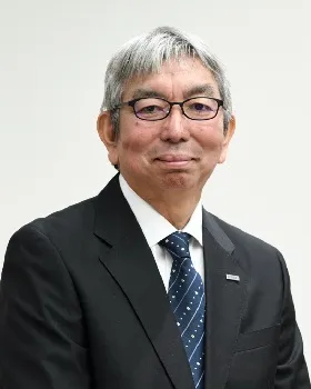
後藤 正人
SCREEN
部署
代表取締役 取締役社長 最高経営責任者(CEO)
AIの進化により半導体需要は飛躍的に拡大する一方、生産性向上や環境負荷低減、人材不足といった新たな課題が生じている。 SCREENが約50年にわたり培ってきた洗浄技術をはじめとする中核技術の進化に加え、アドバンスドパッケージ分野、省エネを中心としたサステナビリティへの取り組みを紹介。 次の50年を支える製造イノベーションの方向性を展望する。
16:10 - 16:40
Beyond the Tester:AI時代の「より複雑に、より速く、より大規模に」への挑戦
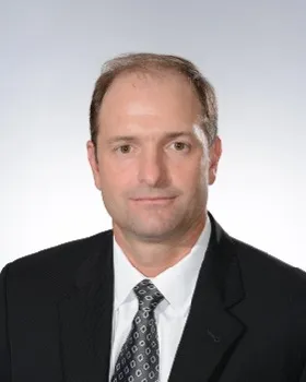
Doug Lefever
Advantest
部署
Group CEO
AIの普及に伴い、半導体デバイスはこれまで以上に高性能化・複雑化し、その開発サイクルは加速を続けると同時に、生産規模もかつてない水準へ拡大しています。このような変化の中で、半導体テストは単なる製造工程の一部ではなく、イノベーションと量産の加速を支える重要な基盤へと進化しつつあります。本講演では、Complexity、Velocity、Scaleという3つの視点から、先端パッケージ、テストセル、データ活用、テスト開発の自動化、そして大規模供給体制といった最新動向を紹介するとともに、半導体テスト市場が今後も成長を続ける構造的な背景と、アドバンテストの戦略的な取り組みについて説明します。
16:40 - 17:00
Atoms, Angstroms, and AI
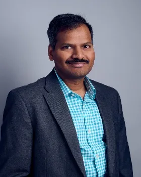
Vamsi Paruchuri
ASM
Corporate Vice President, Technology Innovation & Market Research Organization
役職
The artificial intelligence era is enabled by Angstrom-scale logic and memory technologies built in advanced 3D architectures. As the AI hypercycle accelerates demand for computing performance, semiconductor innovation is increasingly driven by materials engineering, atomic-scale precision, and the ability to manufacture ever more complex structures. Through its leadership in materials innovation and Angstrom-level process control, ASM is defining the next era of semiconductor technology.
Session Sponsors
Stage Sponsors