
HOME
MY PAGE

イベントトップに戻る
セミナースケジュール
Dec.18_11:30_PFAS対策最前線🌿
カテゴリー > 政策・市場
カテゴリー > サステナビリティ
カテゴリー > Dec. 18
カテゴリー > 翻訳サポート
![]() 日英翻訳サポートをご利用希望の方
日英翻訳サポートをご利用希望の方
ご自身のスマートフォンおよびイヤホンをご持参ください。
※詳細はFAQをご確認ください。
昨今PFASの人体・環境への有害性がクローズアップされ、欧米を中心にPFAS規制強化が進められており、製造プロセスでPFAS使用が不可欠な半導体産業では大きな戸惑いが広がっています。本セッションでは、産官学が連携して、PFASに関する解決策を見つけ、持続可能な社会と半導体産業の更なる発展のために果たすべき役割と道筋について議論します。
※プログラムは都合により変更となる場合がございます。予めご了承ください。
プログラムアジェンダ
セッションチェア:
真白 すぴか (SEMI PFAS Initiative)
真白 すぴか (SEMI PFAS Initiative)
11:30-11:45
SEMI及び半導体業界におけるPFAS対策の動向
真白 すぴか
SEMI PFAS Initiative
部署
役職
概要文が入ります。
11:45-12:00
Towards a Greener Future: More Sustainable Materials in Semiconductor Manufacturing
Surésh Rajaraman
Presenter
Executive Vice President and Head of Thin Film Business Unit, and interim Head of Formulations Business Unit and Commercial Leadership Board
The Electronics business of Merck KGaA Darmstadt Germany
GHG emissions and PFAS alternatives are pivotal areas for sustainability efforts in chip manufacturing. In this presentation, Dr. Surésh Rajaraman, EVP and Head of Thin Films Business and interim Head of Formulations and Commercial Leadership Board, will highlight Merck's advancements in identifying alternatives to help solving GHG and PFAS related challenges of the semiconductor industry. We will provide updates on Merck's efforts to identify suitable candidates for PFAS replacement in various applications, such as fluorinated surfactants, EUV anti-collapse rinses, PAGs for chemically amplified photoresists across different wavelengths, and top anti-reflective coatings. And we will share insights into the development of alternative etch gases with significantly reduced atmospheric lifetime, which have the potential to replace traditional etch gases and help reducing GHG emissions in chip manufacturing. Additionally, we will discuss Merck's investment in the Advanced Materials Development Centre in Shizuoka, Japan, where it will explore alternative materials and technological solutions that support more sustainable manufacturing practices.
12:00-12:15
The Sustainable Materials Revolution Driven by IBM Material DX
Alessandro Curioni
IBM Research
IBM Research - Zurich
Europe & Africa and Director
Vice President
IBM Fellow
The semiconductor industry faces unprecedented materials challenges from tightening PFAS regulations, supply chain disruptions, and geopolitical pressures. IBM Material DX addresses these through comprehensive digital transformation, serving as a next-generation R&D platform for semiconductor and materials companies. The solution integrates dispersed data using advanced LLMs and foundation models to accelerate materials discovery and optimize R&D processes. Safe Material Advisor identifies legally risky substances like PFAS in products using AI trained on regulatory and chemical databases. Available on-premise or cloud-deployed to protect proprietary data, IBM Material DX positions companies at the global forefront of industrial innovation.
12:15-12:25
SIPS Japan PFAS WG(1) 実態把握SGの活動について
濱 尚矢
東京エレクトロン
テクノロジービジョン&環境ストラテジー部
役職
SIPS日本部会のPFASワーキンググループにおける実態把握サブグループの活動について報告します。実態把握SGでは、半導体製造工程および設備・製造装置のライフサイクルの中で、どこでどのようなPFASが使用または生成されているかを把握する際に直面する課題を整理しました。また、課題に対する今後の取り組みの方向性についてもあわせて報告します。
12:25-12:35
SIPS Japan PFAS WG(2)リサイクルSGの活動について
淀川 正英
AGC
化学品C 経営戦略本部
パブリックリレーションズ推進室
技術共創推進GL
SIPSの日本部会PFASワーキンググループにおけるリサイクルサブグループの活動について報告します。リサイクルSGでは、フッ素循環に関する業界横断的活動を起草し、循環フッ素社会の実現を提案します。SIPSにおいては、日本のベストプラクティスを示すことを目標に活動してきました。今回その中でもフッ素ポリマーに関わるリサイクルの取り組みを報告します。
12:35-12:45
SIPS Japan PFAS WG(3) 回収・破壊等に関するSGの活動について
大下 真介
ダイキン工業
企画部
渉外担当課長
SIPSの日本部会PFASワーキンググループにおける回収・破壊等に関するサブグループの活動について報告します。PFASの回収・破壊に関しての非網羅的な技術調査と、その実行可能性について報告します。さらに、主要技術の特徴や課題を整理し、実用化に向けた展望や今後の検討課題についても概説します。
12:45-13:00
EU Legislative Framework for Chemicals
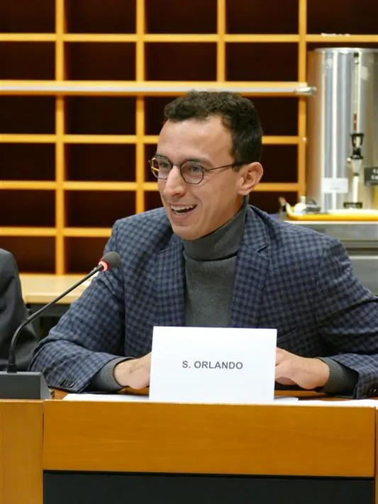
Stefano Ramundo Orlando
Manager
Advocacy and Public Policy
SEMI Europe
The upcoming SEMI Europe presentation will outline the ongoing PFAS Restriction Process under the EU’s REACH regulation and its potential impact on the European semiconductor industry. It will explain how PFAS materials remain essential to chip manufacturing—used in photolithography, plasma etching, sealing, and coating applications—and why viable alternatives are not yet available. SEMI Europe will emphasize the need for a balanced, science-based approach, advocating for critical-use exemptions, realistic transition timelines, and continued dialogue with EU policymakers. The presentation will also highlight SEMI’s ongoing technical engagement and policy advocacy, aiming to ensure that Europe’s competitiveness and innovation capacity are safeguarded as the PFAS restriction process advances.
AI x Sustainability x Semiconductor Summit Emerald Sponsors
AI x Sustainability x Semiconductor Summit Sapphire Sponsors