
HOME
MY PAGE

イベントトップに戻る
セミナースケジュール
Dec.17_15:00_次世代半導体技術2~装置材料編
カテゴリー > SuperTHEATER
カテゴリー > 政策・市場
カテゴリー > 半導体技術
カテゴリー > Dec. 17
カテゴリー > 翻訳サポート
次世代半導体技術2~装置材料編
未来を造る半導体革命
![]()
2025/12/17(水) | 15:00 - 17:00
SuperTHEATER(西4ホール内)
無料
翻訳サポート
![]() 日英翻訳サポートをご利用希望の方
日英翻訳サポートをご利用希望の方
ご自身のスマートフォンおよびイヤホンをご持参ください。
※詳細はFAQをご確認ください。
半導体の微細化・高性能化・三次元化が加速する中で、装置と材料の革新はますます重要性を増しています。 本セッションでは、最先端の露光・加工・パッケージング技術、そしてそれらを支える高機能材料に焦点を当て、 業界をけん引する企業が次世代に向けた取り組みを紹介し、これらの分野をリードするトップ企業が集結します。 装置と材料の両面から、グローバル競争を勝ち抜く半導体製造の技術動向と未来を探ります。
※プログラムは都合により変更となる場合がございます。予めご了承ください。
プログラムアジェンダ
15:00 - 15:30
How Deposition and Etch Are Reshaping the 3D Era
Vahid Vahedi
Lam Research
Senior Vice President, Chief Technology and Sustainability Officer
役職
AI is fueling unprecedented growth and accelerating demand for advanced devices. Its requirements for performance, power, and area scaling are driving memory and logic devices toward 3D architectures. At the heart of this 3D transformation, processing steps must enable taller, perpendicular structures as well as smaller features. Meeting these requirements calls for new deposition and etch capabilities that did not exist before, leading to breakthroughs needed in areas such as atomic-level deposition and etch (ALD and ALE), high-aspect-ratio processing, dry resist EUV patterning, and the adoption of new materials like molybdenum (Mo). As a result, the transition to 3D devices will drive increased intensity of deposition and etch processing. This presentation will explore how deposition and etch are critical to unlocking the future of 3D devices, with increasing velocity required to meet the demands of AI-driven innovation.
15:30 - 16:00
AI時代を支える先端材料の挑戦
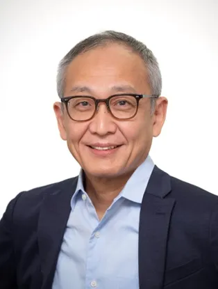
菅原 静郎
JX金属
取締役副社長執行役員
生成AIの普及化以降データ産業は進化が一層加速している。材料メーカーにおいても、各企業個々の努力だけでなく、今後は益々企業同士や研究機関との連携により進化に伴う技術課題や社会課題への解決策を提示していかなければならない。本解決に向けた当社におけるデータインフラ材料の開発動向と、サプライチェーンの強化策について紹介する。
16:00 - 16:30
AI共創と最先端材料で拓く次世代半導体製造
岩﨑 哲也
富士フイルム
取締役・常務執行役員 エレクトロニクスマテリアルズ事業部⾧
役職
富士フイルムは、前工程のみならず後工程までのほぼ全ての製造プロセスにおいて、幅広い製品を提供する「ワンストップソリューション」を展開しています。本講演では製品特長や事業戦略、AI技術を梃にした他社や顧客との共創事例、そして超先端材料による次世代半導体製造への貢献事例をお伝えします。
16:30 - 17:00
AI時代のKiru・Kezuru・Migaku
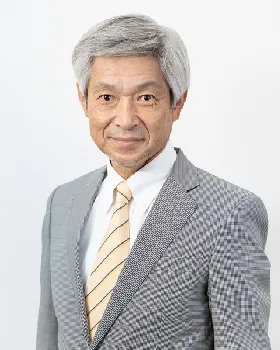
吉永 晃
ディスコ
取締役 代表執行役副社長 営業本部長
AI時代の半導体ではパッケージの進化に伴い、グラインディングやダイシング工程のイノベーションが求められる。
当社ではこれら工程を「中工程」と位置づけ、加工品質と歩留まりの向上に貢献している。
本講演では、先端パッケージにおける当社の技術と自動化への取り組みを紹介する。
Stage Sponsors